
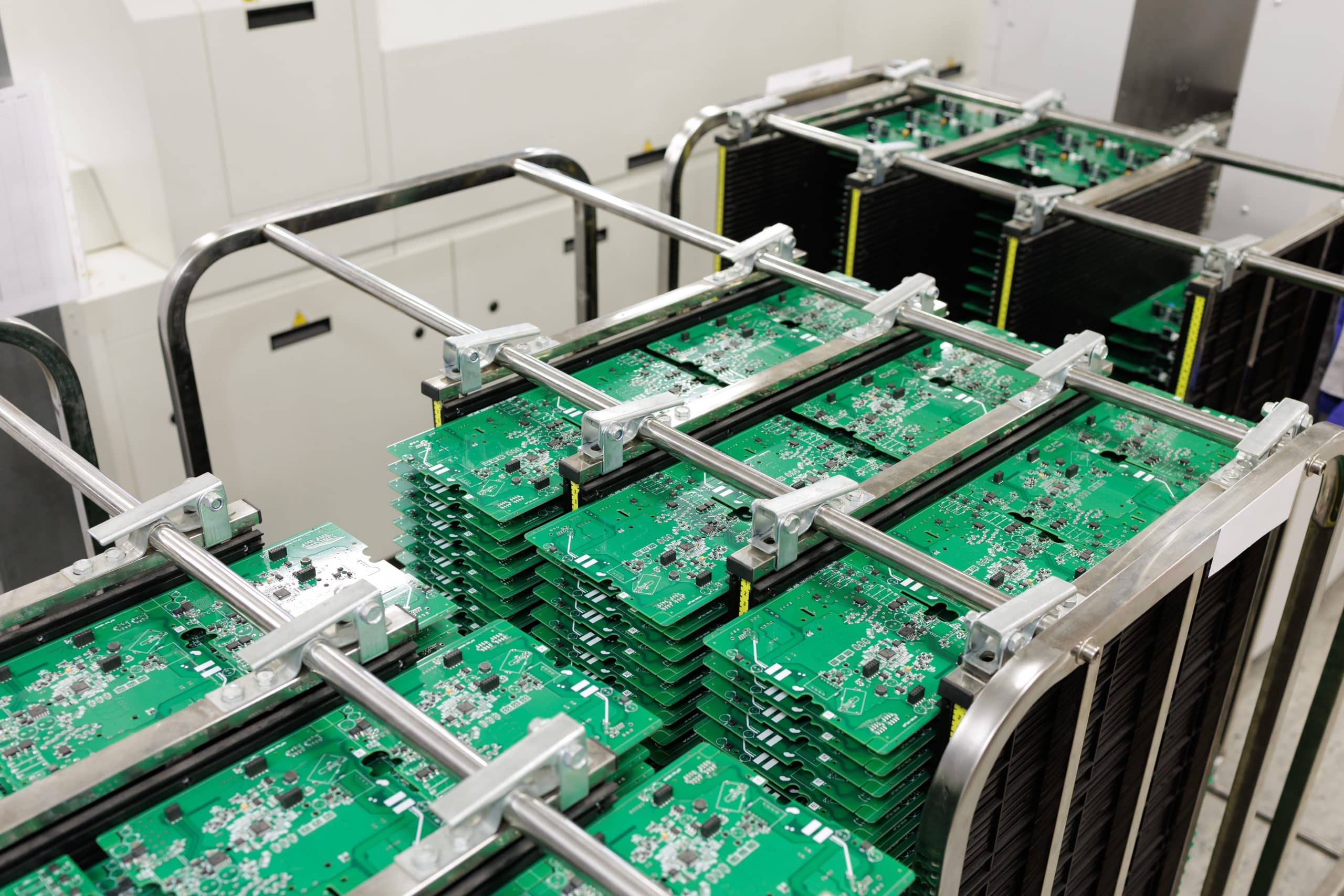
In high-density SMT assembly, even small variations in solder paste release can lead to print defects, inconsistent deposits, increased cleaning downtime, and yield instability. When these issues appear, the investigation typically focuses on paste type, stencil thickness, or aperture geometry. What is often overlooked is the stencil surface itself and how the coating applied to it influences paste behavior during every print cycle.
Understanding how nanocoatings for SMT stencils compare to traditional surface treatments helps process engineers make more informed decisions when optimizing stencil performance for demanding applications.
What Traditional Coatings Do
Before nanocoatings became widely available, the primary post-processing option for improving stencil surface performance was electropolishing. Electropolishing is an electrochemical process that smooths the aperture walls of a laser cut stencil by removing a thin layer of material from the surface. This reduces surface roughness, which in turn improves paste release and reduces residue buildup inside apertures.
Electropolishing remains a valid and effective post-processing technique, particularly for applications where aperture wall smoothness is the primary concern. However, it addresses surface texture rather than surface chemistry. It does not fundamentally change how the stencil surface interacts with solder paste during printing.
How Nanocoatings Work
Nanocoatings take a different approach. Rather than removing material to smooth the surface, a nanocoating applies an ultra-thin layer of material to the stencil surface that alters its chemical properties. The result is a surface with lower solder paste adhesion rather than simply a smoother aperture profile.
The paste separates more cleanly from the aperture walls during the print stroke, leaving less residue behind and maintaining more consistent deposit volumes across the board. The effect is particularly significant for fine-pitch features and small apertures where clean release is hardest to achieve and most critical to yield.
Nanocoatings also reduce the rate at which paste residue accumulates inside apertures between cleaning cycles. In high-volume production environments, this translates to more stable print performance over longer runs and less frequent downtime for stencil cleaning.
Performance Comparison
When comparing nanocoatings to electropolishing across key performance indicators, the differences become especially meaningful in precision SMT applications.
In terms of paste transfer efficiency, nanocoatings typically outperform uncoated and electropolished stencils at low area ratios, where aperture geometry makes clean release inherently more difficult. For designs operating near or below the 0.66 area ratio threshold, nanocoatings can improve transfer efficiency beyond what is typically achievable with electropolishing alone.
For aperture cleanliness over extended runs, nanocoatings maintain more consistent performance between cleaning cycles. Electropolished stencils improve initial paste release but do not reduce residue accumulation at the same rate as nanocoated surfaces over extended production runs.
Nanocoatings may also help reduce wear-related surface degradation over time by limiting residue buildup and reducing repeated mechanical interaction during cleaning cycles.
When Nanocoatings Make the Most Difference
Nanocoatings deliver the greatest performance benefit in applications where:
- Fine-pitch components or small apertures push area ratios toward or below the practical minimum for reliable paste transfer
- High-volume production runs require stable, consistent print performance between cleaning cycles
- Mixed-component boards include both small and large features, where paste release consistency across varying aperture sizes is critical
- Process margins are already tight and small variations in paste volume directly affect yield
For less demanding applications with larger aperture sizes and more forgiving tolerances, electropolishing may be sufficient. However, as PCB designs continue to shrink and process demands increase, the performance advantages of nanocoatings become increasingly relevant across a wider range of SMT applications.
Choosing the Right Surface Treatment
Electropolishing and nanocoatings are not mutually exclusive. In some cases, combining both treatments produces the best results. Electropolishing addresses surface roughness at the aperture wall level, while the nanocoating addresses surface chemistry and solder paste adhesion behavior.
For many high-precision SMT applications, nanocoatings for SMT stencils represent a more effective approach to improving paste release consistency and process stability across extended production runs. Selecting the right surface treatment alongside stencil thickness, aperture design, and material selection is part of building a stencil printing process that performs reliably at scale.
Every SMT process has different demands. Whether you are evaluating nanocoatings for a fine-pitch application, managing cleaning cycle frequency in high-volume production, or specifying a new stencil from scratch, MicroScreen can help identify the right surface treatment for your process. Contact MicroScreen to discuss the right surface treatment for your stencil application.